Kontakt
 Jak nakupovat
Doručení
Nákupní rádce
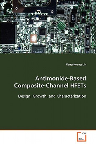
Antimonide-Based Composite-Channel HFETs
 Angličtina
 119 b
119 b
Až 30 dní na vrácení zboží
Zákazníci také koupili


The binary compound semiconductors, InSb and InAs,along with their related alloys with similar latticeconstants are candidates for high-speed, low-powerelectronic devices. Applications could include high-speed analog and digital systems used for dataprocessing, communications, imaging, and sensing,particularly in portable equipment such as hand-helddevices and satellites. The development of Sb-basedtransistors for use in low-noise high-frequencyamplifiers, digital circuits, and mixed-signalcircuits could provide the enabling technologyneeded to address these rapidly expanding needs.However, a drawback of the technology is the lowbreakdown voltage associated with the relativelynarrow band-gap InAs channel. Added with staggeredband lineup at InAs/AlSb heterojunction, thegenerated holes from the breakdown cannot beconfined in the channel and result in significanteffects on device performance. In this work, wepropose an alternative approach of composite channelto alleviate this issue. Device design, growth,fabrication and characterization will be describedin details.


Informace o knize
Angličtina

Darujte tuto knihu ještě dnes
Je to snadné
1 Přidejte knihu do košíku a zvolte doručit jako dárek 2 Obratem vám zašleme poukaz 3 Kniha dorazí na adresu obdarovanéhoMohlo by vás také zajímat
 /
/
 Brožovaná
 532
Kč
532
Kč
 /
Brožovaná
336
Kč
/
Brožovaná
336
Kč


 /
Brožovaná
444
Kč
/
Brožovaná
444
Kč
 /
Brožovaná
175
Kč
/
Brožovaná
175
Kč